|
The laser is one of the core optoelectronic devices for silicon-based photonic integration and has been one of the research hotspots of silicon-based photonics. The integration of the silicon-based laser with the silicon-based waveguide device provides a light source. In 2009, our group's researcher Dr. Chu Tao successively developed the world's first silicon-based wavelength tunable laser and the 100nm adjustable range widest laser. In 2014, the group successfully developed silicon-based hybrid integrated lasers with self-made high-precision chip bonding equipment, with an output power of 4.2mW. This is the first time in China that a mixture of III-V series lasers and silicon-based photonic devices fabricated by standard CMOS processes has been realized. It has laid the foundation for the fabrication of silicon-based lasers using CMOS line scale.
|
|
The main implementation directions of silicon-based lasers are as follows: 1. Using flip-chip bonding technology, integrate the separately fabricated III-V devices and silicon-based devices; 2. Bonding III-V materials on SOI wafers, and then make the device. The scheme 1 has advantages in cost and device performance. The LD is coupled by the end face coupling and the silicon-based waveguide, and for alignment assembly and corresponding equipment, the alignment accuracy should be controlled strictly less than ±0.5μm. Option 2 has an advantage in wafer level processing. Japan's PETRA, NEC and Fujitsu companies, Europe's IMEC and Ghent universities, the United States' Intel and UCSB conducted research on silicon-based lasers in the above two ways. Japan and Germany mainly adopt option 1, while IMEC and US intel are more inclined. Study in scenario 2.
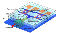
In 2009, In 2009, the researcher of our group, using the thermal light effect of silicon material and the Vernier effect of micro-ring resonator, successfully developed the world's first silicon-based wavelength tunable laser with the widest wavelength range. And the wavelength tuning range is up to 100nm, the output power is up to 12mW.
,
|
|
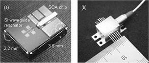
In December 2014, we fabricated silicon-based photonic device substrates respectively using EB process and 0.18μm-CMOS process, and realized monolithic integration of III-V lasers with silicon-based photonic devices using self-made high-precision infrared alignment bonding devices. Its coupling loss is less than 3dB and maximum output power is up to 4.2mW. For the first time in China, the hybrid integration of III-V lasers with silicon-based photonic device substrates fabricated by standard CMOS processes has been realized, marking the possibility of mass-produced silicon-based lasers using standard CMOS lines.
|